Analytical services


Assuring the cleanliness of the manufacturing environment
The process for manufacturing electronics components such as flat panel displays or photovoltaic cells can involve up to 20 different process steps and last multiple days. For semiconductors, this process involves up to 250 steps and can take several months.
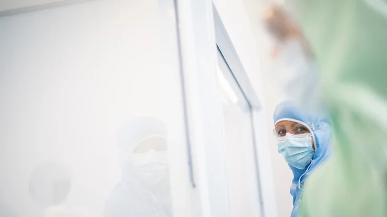
Regardless of the duration, we know it is imperative to maintain clean manufacturing discipline, cleanliness of the fab environment and avoid any detrimental trace or particle level contaminants at the process level that could alter or ruin the performances of the electronic components or the fab throughputs. The challenge is acute with semiconductors, where the smallest elements approach just a few atom layers in thickness.
Comprehensive analytical services
Air Liquide offers comprehensive analytical services through our Balazs™ NanoAnalysis and Toshiba Nanoanalysis subsidiaries.
Ensuring clean manufacturing procedures
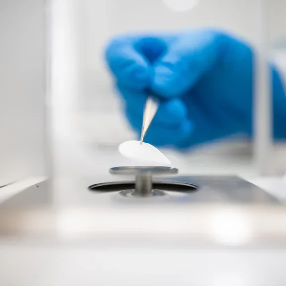
These services ensure the purity of starting materials, consumables, process tool components, cleanroom environment and clean manufacturing procedures meet the requirement to manufacture high-technology products. Our expertise extends to contamination problem solving to trace back any detected contamination to the root source. Our goal is to help customers improve their yield and to develop and implement faster next generation technologies.
To this end our services include:
- Failure analysis and Yield improvement
- Contamination reduction
- Process optimization
- Materials cleanliness testing
- Film and coating characterization
- Analytical testing, planning and consulting
- Clean manufacturing training and onsite gap analysis
Balazs™ NanoAnalysis is headquartered in Fremont, California (U.S.) with additional facilities in Dallas, Texas (U.S.) and Crolles (France). Toshiba Nanoanalysis is a joint-venture between Toshiba and Air Liquide with its headquarters in Japan.
Maintaining confidentiality is of paramount concern. Balazs™ NanoAnalysis and Toshiba Nanoanalysis are both independent laboratories and fiercely protect client data and proprietary information.